Difference between revisions of "Argon user guide/J5 connector electrical interfacing"
From Granite Devices Knowledge Wiki
| [checked revision] | [checked revision] |
(→High speed digital input) |
|||
| Line 14: | Line 14: | ||
===High speed digital input=== | ===High speed digital input=== | ||
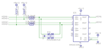
| − | [[File:hsin.png|thumb| | + | [[File:hsin.png|thumb|Simplified HSIN circuity inside the drive. Left side end represents J5 pins and right side continues to drive internal circuity.]] |
HSIN is differential digital input capable of receiving digital signals up to 4 MHz. | HSIN is differential digital input capable of receiving digital signals up to 4 MHz. | ||
| Line 34: | Line 34: | ||
===Analog input=== | ===Analog input=== | ||
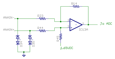
| + | [[File:anain.png|thumb|Simplified analog input circuity inside the drive. Left side end represents J5 pins and right side continues to drive internal circuits.]] | ||
===Digital output=== | ===Digital output=== | ||
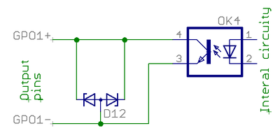
| + | [[File:gpo.png|thumb|Simplified digital output circuity inside the drive. Left side end represents J5 pins and right side continues to drive internal circuits.]] | ||
===Digital input=== | ===Digital input=== | ||
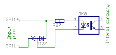
| + | [[File:gpi.png|thumb|Simplified digital input circuity inside the drive. Left side end represents J5 pins and right side continues to drive internal circuits. D27 protects optocoupler from reverse polarity and ESD.]] | ||
[[Category:Argon]] | [[Category:Argon]] | ||
[[Category:Setup guides]] | [[Category:Setup guides]] | ||
[[Category:Unfinished]] | [[Category:Unfinished]] | ||
Revision as of 17:22, 14 June 2013
This article explains the internal circuity behind J5 connector of Argon servo drive.
| Exceeding ratings may affect drive operation and cause instability or even damage the drive. |
Contents
Pin electrical categories
Supply
Supply pins output a regulated 5V voltage to external circuits. GND pin is tied to J3 connector V- terminal.
- Electrical properties
- Output voltage 4.9-5.2 V
- Maximum load 500 mA
- Maximum injected current -10 mA
| Never connect multiple supply outputs parallel. Supply output may be connected only current consuming circuity to prevent current injection to the supply port. |
High speed digital input
HSIN is differential digital input capable of receiving digital signals up to 4 MHz.
- Electrical properties
- Maximum voltage to +/- pins referenced to GND: -0.5 to 6V. Nominal 3.3 or 5.0V.
- Maximum injected current +/- 10 mA
- When negative input (-) is left floating, it floats around 2.5V
- Input state is logic 1 when voltage on positive pin is greater than voltage on negative pin, otherwise it's logic 0
- Wiring when driving using differential source
- Positive (+) inputs: to positive outputs of source
- Negative (-) inputs: to negative outputs of source
- GND must be connected to source ground
- Wiring when driving using single ended source (TTL, CMOS or open collector)
- Positive (+) inputs: to outputs of source
- Negative (-) inputs: leave floating
- GND must be connected to source ground


