Difference between revisions of "Argon user guide/J5 connector electrical interfacing"
From Granite Devices Knowledge Wiki
| [checked revision] | [checked revision] |
| Line 18: | Line 18: | ||
;Electrical properties | ;Electrical properties | ||
| − | *Maximum voltage to +/- pins referenced to GND: -0.5 to 6V. Nominal 3.3 or 5.0V. | + | *Maximum voltage to HSINx+/- pins referenced to GND: -0.5 to 6V. Nominal 3.3 or 5.0V. |
*Maximum injected current +/- 10 mA | *Maximum injected current +/- 10 mA | ||
| − | *When negative input (-) is left floating, it floats around 2.5V | + | *When negative input (HSINx-) is left floating, it floats around 2.5V |
*Input state is logic 1 when voltage on positive pin is greater than voltage on negative pin, otherwise it's logic 0 | *Input state is logic 1 when voltage on positive pin is greater than voltage on negative pin, otherwise it's logic 0 | ||
;Wiring when driving using differential source | ;Wiring when driving using differential source | ||
| − | *Positive | + | *Positive outputs of source to HSINx+ |
| − | *Negative | + | *Negative outputs of source to HSINx- |
*GND must be connected to source ground | *GND must be connected to source ground | ||
;Wiring when driving using single ended source (TTL, CMOS or open collector) | ;Wiring when driving using single ended source (TTL, CMOS or open collector) | ||
| − | * | + | *Outputs of source to HSINx+ |
| − | * | + | *Leave HSINx- floating |
*GND must be connected to source ground | *GND must be connected to source ground | ||
| Line 38: | Line 38: | ||
;Electrical properties | ;Electrical properties | ||
*Input impedance ~10 kΩ | *Input impedance ~10 kΩ | ||
| − | *Maximum +/- pin voltage vs GND ±20V | + | *Maximum ANAINx+/- pin voltage vs GND ±20V |
*Maximum injected current ±10 mA | *Maximum injected current ±10 mA | ||
*Sampling resolution 12 bits | *Sampling resolution 12 bits | ||
;Wiring to differential signal source | ;Wiring to differential signal source | ||
| − | *Connect positive output to | + | *Connect positive output to ANAINx+ |
| − | *Connect negative (inverted) output to | + | *Connect negative (inverted) output to ANAINx- |
*Connect source ground to GND | *Connect source ground to GND | ||
;Wiring to single ended signal source | ;Wiring to single ended signal source | ||
| − | *Connect output to | + | *Connect output to ANAINx+ |
| − | *Connect source ground to | + | *Connect source ground to ANAINx- |
*Connect source ground to GND | *Connect source ground to GND | ||
| Line 56: | Line 56: | ||
*Load voltage range 3-24V | *Load voltage range 3-24V | ||
*Maximum allowed load 50 mA | *Maximum allowed load 50 mA | ||
| − | *Logic 1 state equals conducting state of optocoupler transistor (current flows from + to - pins), logic 0 stops current flow between + to - pins. | + | *Logic 1 state equals conducting state of optocoupler transistor (current flows from GPO+ to GPO- pins), logic 0 stops current flow between GPO+ to GPO- pins. |
*+ to - pin voltage drop at 50 mA less than 2 VDC | *+ to - pin voltage drop at 50 mA less than 2 VDC | ||
{{caution|Digital output isolation is only functional and does not provide safety insulation. Connect only to [http://en.wikipedia.org/wiki/Extra-low_voltage ELV circuits].}} | {{caution|Digital output isolation is only functional and does not provide safety insulation. Connect only to [http://en.wikipedia.org/wiki/Extra-low_voltage ELV circuits].}} | ||
| Line 69: | Line 69: | ||
*Logic 0 when difference between +/- inputs less than 1.5V, logic 0 when more than 2.9V | *Logic 0 when difference between +/- inputs less than 1.5V, logic 0 when more than 2.9V | ||
*Current needed to drive logic 1 is 0.8-9 mA depending on input voltage | *Current needed to drive logic 1 is 0.8-9 mA depending on input voltage | ||
| − | *Maximum voltage difference between +/- inputs 27 VDC | + | *Maximum voltage difference between GPIx+/- inputs 27 VDC |
| − | *Maximum voltage difference between +/- inputs vs GND 120 VDC | + | *Maximum voltage difference between GPIx+/- inputs vs GND 120 VDC |
{{caution|Digital input isolation is only functional and does not provide safety insulation. Connect only to [http://en.wikipedia.org/wiki/Extra-low_voltage ELV circuits].}} | {{caution|Digital input isolation is only functional and does not provide safety insulation. Connect only to [http://en.wikipedia.org/wiki/Extra-low_voltage ELV circuits].}} | ||
;Connection to electromechanical switch or relay | ;Connection to electromechanical switch or relay | ||
| Line 76: | Line 76: | ||
*See schematics image in right side | *See schematics image in right side | ||
;Connection to CMOS source | ;Connection to CMOS source | ||
| − | *Connect source output to | + | *Connect source output to GPIx+ input |
| − | *Connect source ground to | + | *Connect source ground to GPIx- input |
;Connection to open collector or TTL source | ;Connection to open collector or TTL source | ||
| − | *Connect source output to | + | *Connect source output to GPIx- input |
| − | *Connect source VCC (typ 5V) to | + | *Connect source VCC (typ 5V) to GPOx+ input |
[[Category:Argon]] | [[Category:Argon]] | ||
[[Category:Setup guides]] | [[Category:Setup guides]] | ||
[[Category:Unfinished]] | [[Category:Unfinished]] | ||
Revision as of 19:28, 14 June 2013
This article explains the internal circuity behind J5 connector of Argon servo drive.
| Exceeding ratings may affect drive operation and cause instability or even damage the drive. |
Contents
Pin electrical categories
Supply
Supply pins output a regulated 5V voltage to external circuits. GND pin is tied to J3 connector V- terminal.
- Electrical properties
- Output voltage 4.9-5.2 V
- Maximum load 500 mA
- Maximum injected current -10 mA
| Never connect multiple supply outputs parallel. Supply output may be connected only current consuming circuity to prevent current injection to the supply port. |
High speed digital input
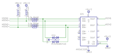
HSIN is differential digital input capable of receiving digital signals up to 4 MHz.
- Electrical properties
- Maximum voltage to HSINx+/- pins referenced to GND: -0.5 to 6V. Nominal 3.3 or 5.0V.
- Maximum injected current +/- 10 mA
- When negative input (HSINx-) is left floating, it floats around 2.5V
- Input state is logic 1 when voltage on positive pin is greater than voltage on negative pin, otherwise it's logic 0
- Wiring when driving using differential source
- Positive outputs of source to HSINx+
- Negative outputs of source to HSINx-
- GND must be connected to source ground
- Wiring when driving using single ended source (TTL, CMOS or open collector)
- Outputs of source to HSINx+
- Leave HSINx- floating
- GND must be connected to source ground
Analog input
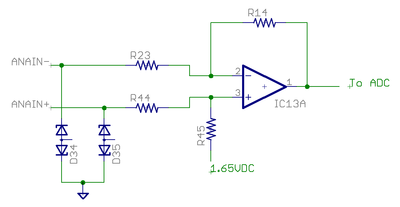
Analog input accepts ±10V from and may be used as reference signal.
- Electrical properties
- Input impedance ~10 kΩ
- Maximum ANAINx+/- pin voltage vs GND ±20V
- Maximum injected current ±10 mA
- Sampling resolution 12 bits
- Wiring to differential signal source
- Connect positive output to ANAINx+
- Connect negative (inverted) output to ANAINx-
- Connect source ground to GND
- Wiring to single ended signal source
- Connect output to ANAINx+
- Connect source ground to ANAINx-
- Connect source ground to GND
Digital output
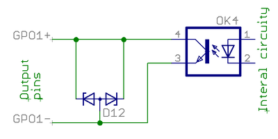
Digital output is an optoisolated transistor output to drive various types of inputs of target devices (logic gates, relays, lights etc)
- Electrical properties
- Load voltage range 3-24V
- Maximum allowed load 50 mA
- Logic 1 state equals conducting state of optocoupler transistor (current flows from GPO+ to GPO- pins), logic 0 stops current flow between GPO+ to GPO- pins.
- + to - pin voltage drop at 50 mA less than 2 VDC
| Digital output isolation is only functional and does not provide safety insulation. Connect only to ELV circuits. |
- Wiring to logic gate input (CMOS or TTL)
- Connect GPO+ pin to target VCC (typ 5V)
- Connect GPO- pin to target input pin (so input pin is pulled to 5V when output state is logic 1)
Digital input
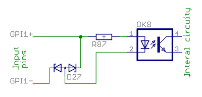
Digital inputs are optoisolated (floating potential) inputs for general purpose control signals.
- Electrical properties
- Signal voltage range 3-24V
- Logic 0 when difference between +/- inputs less than 1.5V, logic 0 when more than 2.9V
- Current needed to drive logic 1 is 0.8-9 mA depending on input voltage
- Maximum voltage difference between GPIx+/- inputs 27 VDC
- Maximum voltage difference between GPIx+/- inputs vs GND 120 VDC
| Digital input isolation is only functional and does not provide safety insulation. Connect only to ELV circuits. |
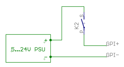
- Connection to electromechanical switch or relay
- See schematics image in right side
- Connection to CMOS source
- Connect source output to GPIx+ input
- Connect source ground to GPIx- input
- Connection to open collector or TTL source
- Connect source output to GPIx- input
- Connect source VCC (typ 5V) to GPOx+ input
