Difference between revisions of "IONI connector pinout"
From Granite Devices Knowledge Wiki
| [checked revision] | [checked revision] |
| Line 70: | Line 70: | ||
|} | |} | ||
Note: pins marked as ''Not connected'' are left empty for to make larger clearance for high voltage signals. Leave these pins unconnected on motherboard designs. | Note: pins marked as ''Not connected'' are left empty for to make larger clearance for high voltage signals. Leave these pins unconnected on motherboard designs. | ||
| + | [[category:Ioni]] | ||
| + | [[category:Ioni user guide]] | ||
Revision as of 14:51, 6 February 2015
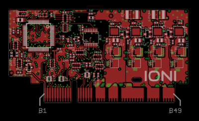
IONI card edge connector fits into a standard PCI-Express 8X socket connector. The pinout of IONI drive is provided in the following table.
- I/O and low voltage signals
| Pin | Signal name | Pin | Signal name | |
|---|---|---|---|---|
| A1 | GND | B1 | 5V_IN | |
| A2 | RS485_A | B2 | RS485_B | |
| A3 | ADDRSEL1 | B3 | ADDRSEL2 | |
| A4 | HSIN1 | B4 | HSIN2 | |
| A5 | ANAIN- | B5 | ANAIN+ | |
| A6 | GPI1 | B6 | GPI2 | |
| A7 | GPI3 | B7 | GPI4 | |
| A8 | GPO1 | B8 | GPO2 | |
| A9 | GPO3 | B9 | GPO4 | |
| A10 | GPO5 | B10 | GPO6 | |
| A11 | REGEN_OUT | B11 | MECH_BRAKE_OUT | |
| A12 | ENABLE_IN | B12 | Reserved/NC | |
| A13 | STO2 | B13 | HALL_W | |
| A14 | HALL_V | B14 | HALL_U | |
| A15 | CHA- | B15 | CHA+ | |
| A16 | CHB- | B16 | CHB- | |
| A17 | CHC- | B17 | CHC- |
- Power signals
| Pin | Signal name | Pin | Signal name | |
|---|---|---|---|---|
| A18-A22 | GND | B18 | Not connected | |
| A23 | Not connected | B19-B22 | HV+ | |
| A24-A27 | PHASE1 | B23 | Not connected | |
| A28 | Not connected | B24-B27 | PHASE2 | |
| A29-A37 | PHASE3 | B28 | Not connected | |
| A38 | Not connected | B29-B37 | PHASE4 | |
| A39-A43 | PHASE1 | B38 | Not connected | |
| A44 | Not connected | B39-B43 | PHASE2 | |
| A45-A49 | GND | B44 | Not connected | |
| B45-B49 | HV+ |
Note: pins marked as Not connected are left empty for to make larger clearance for high voltage signals. Leave these pins unconnected on motherboard designs.
