Difference between revisions of "Argon user guide/J5 connector electrical interfacing"
From Granite Devices Knowledge Wiki
| [checked revision] | [checked revision] |
| Line 59: | Line 59: | ||
*Logic 1 state equals conducting state of optocoupler transistor (current flows from GPO+ to GPO- pins), logic 0 stops current flow between GPO+ to GPO- pins. | *Logic 1 state equals conducting state of optocoupler transistor (current flows from GPO+ to GPO- pins), logic 0 stops current flow between GPO+ to GPO- pins. | ||
*+ to - pin voltage drop at 50 mA less than 2 VDC | *+ to - pin voltage drop at 50 mA less than 2 VDC | ||
| − | |||
;Wiring to logic gate input (CMOS or TTL) | ;Wiring to logic gate input (CMOS or TTL) | ||
*Connect GPO+ pin to target VCC (typ 5V) | *Connect GPO+ pin to target VCC (typ 5V) | ||
*Connect GPO- pin to target input pin (so input pin is pulled to 5V when output state is logic 1) | *Connect GPO- pin to target input pin (so input pin is pulled to 5V when output state is logic 1) | ||
| + | {{caution|Digital output isolation is only functional and does not provide safety insulation. Connect only to [http://en.wikipedia.org/wiki/Extra-low_voltage ELV circuits].}} | ||
===Digital input=== | ===Digital input=== | ||
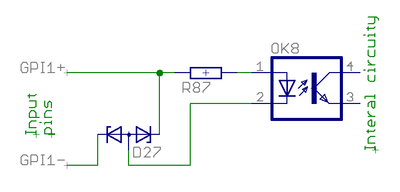
[[File:gpi.png|thumb|Simplified digital input circuity inside the drive. Left side end represents J5 pins and right side continues to drive internal circuits. D27 protects optocoupler from reverse polarity and ESD.]] | [[File:gpi.png|thumb|Simplified digital input circuity inside the drive. Left side end represents J5 pins and right side continues to drive internal circuits. D27 protects optocoupler from reverse polarity and ESD.]] | ||
| Line 72: | Line 72: | ||
*Maximum voltage difference between GPIx+/- inputs 27 VDC | *Maximum voltage difference between GPIx+/- inputs 27 VDC | ||
*Maximum voltage difference between GPIx+/- inputs vs GND 120 VDC | *Maximum voltage difference between GPIx+/- inputs vs GND 120 VDC | ||
| − | |||
;Connection to electromechanical switch or relay | ;Connection to electromechanical switch or relay | ||
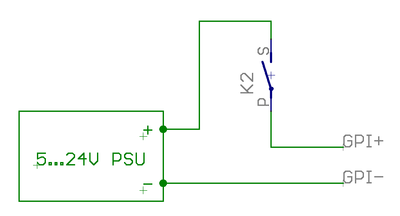
[[File:gpiswitch.png|thumb|Connection from electromechanical switch or relay to isolated digital input. PSU may be external power supply or 5V supply from J5 connector.]] | [[File:gpiswitch.png|thumb|Connection from electromechanical switch or relay to isolated digital input. PSU may be external power supply or 5V supply from J5 connector.]] | ||
| Line 82: | Line 81: | ||
*Connect source output to GPIx- input | *Connect source output to GPIx- input | ||
*Connect source VCC (typ 5V) to GPOx+ input | *Connect source VCC (typ 5V) to GPOx+ input | ||
| + | {{caution|Digital input isolation is only functional and does not provide safety insulation. Connect only to [http://en.wikipedia.org/wiki/Extra-low_voltage ELV circuits].}} | ||
[[Category:Argon]] | [[Category:Argon]] | ||
[[Category:Setup guides]] | [[Category:Setup guides]] | ||
| − | |||
Revision as of 19:25, 15 June 2013
This article explains the internal circuity behind J5 connector of Argon servo drive.
| Exceeding ratings may affect drive operation and cause instability or even damage the drive. |
Contents
Pin functions
See main article Argon wiring
Pin electrical categories
Supply
Supply pins output a regulated 5V voltage to external circuits. GND pin is tied to J3 connector V- terminal.
- Electrical properties
- Output voltage 4.9-5.2 V
- Maximum load 500 mA
- Maximum injected current -10 mA
| Never connect multiple supply outputs parallel. Supply output may be connected only current consuming circuity to prevent current injection to the supply port. |
High speed digital input
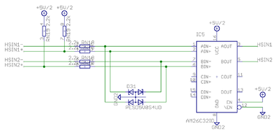
HSIN is differential digital input capable of receiving digital signals up to 4 MHz.
- Electrical properties
- Maximum voltage to HSINx+/- pins referenced to GND: -0.5 to 6V. Nominal 3.3 or 5.0V.
- Maximum injected current +/- 10 mA
- When negative input (HSINx-) is left floating, it floats around 2.5V
- Input state is logic 1 when voltage on positive pin is greater than voltage on negative pin, otherwise it's logic 0
- Wiring when driving using differential source
- Positive outputs of source to HSINx+
- Negative outputs of source to HSINx-
- GND must be connected to source ground
- Wiring when driving using single ended source (TTL, CMOS or open collector)
- Outputs of source to HSINx+
- Leave HSINx- floating
- GND must be connected to source ground
Analog input
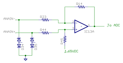
Analog input accepts ±10V from and may be used as reference signal.
- Electrical properties
- Input impedance ~10 kΩ
- Maximum ANAINx+/- pin voltage vs GND ±20V
- Maximum injected current ±10 mA
- Sampling resolution 12 bits
- Wiring to differential signal source
- Connect positive output to ANAINx+
- Connect negative (inverted) output to ANAINx-
- Connect source ground to GND
- Wiring to single ended signal source
- Connect output to ANAINx+
- Connect source ground to ANAINx-
- Connect source ground to GND
Digital output
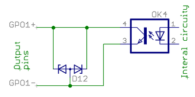
Digital output is an optoisolated transistor output to drive various types of inputs of target devices (logic gates, relays, lights etc)
- Electrical properties
- Load voltage range 3-24V
- Maximum allowed load 50 mA
- Logic 1 state equals conducting state of optocoupler transistor (current flows from GPO+ to GPO- pins), logic 0 stops current flow between GPO+ to GPO- pins.
- + to - pin voltage drop at 50 mA less than 2 VDC
- Wiring to logic gate input (CMOS or TTL)
- Connect GPO+ pin to target VCC (typ 5V)
- Connect GPO- pin to target input pin (so input pin is pulled to 5V when output state is logic 1)
| Digital output isolation is only functional and does not provide safety insulation. Connect only to ELV circuits. |
Digital input
Digital inputs are optoisolated (floating potential) inputs for general purpose control signals.
- Electrical properties
- Signal voltage range 3-24V
- Logic 0 when difference between +/- inputs less than 1.5V, logic 0 when more than 2.9V
- Current needed to drive logic 1 is 0.8-9 mA depending on input voltage
- Maximum voltage difference between GPIx+/- inputs 27 VDC
- Maximum voltage difference between GPIx+/- inputs vs GND 120 VDC
- Connection to electromechanical switch or relay
- See schematics image in right side
- Connection to CMOS source
- Connect source output to GPIx+ input
- Connect source ground to GPIx- input
- Connection to open collector or TTL source
- Connect source output to GPIx- input
- Connect source VCC (typ 5V) to GPOx+ input
| Digital input isolation is only functional and does not provide safety insulation. Connect only to ELV circuits. |
