Difference between revisions of "IONICUBE connectors and pinouts"
| [checked revision] | [checked revision] |
(→Front side connectors) |
(→X4 pinout) |
||
| (21 intermediate revisions by 2 users not shown) | |||
| Line 28: | Line 28: | ||
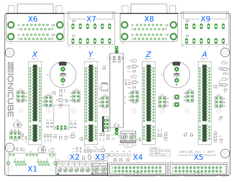
{{picturebox|Ionicubelayout.png|caption=Connector layout and naming. View from top of the board.}} | {{picturebox|Ionicubelayout.png|caption=Connector layout and naming. View from top of the board.}} | ||
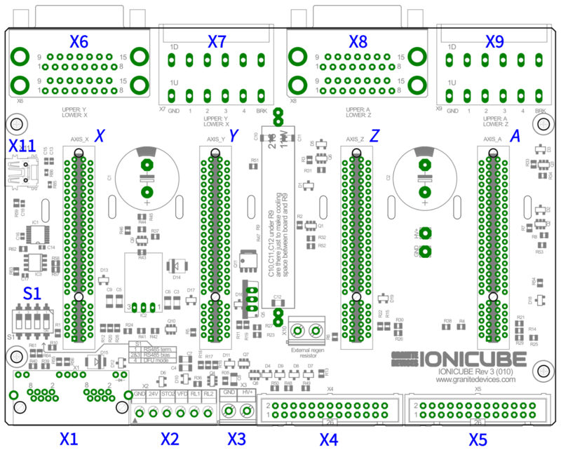
| + | {{picturebox|Ionicube revision 3 layout.png|caption=IONICUBE revision 3 PCB layout. USB connector X11 and Switch S1 to replace the jumper header.}} | ||
| − | {{picturebox|Ioni motoroutouts per drive.png|caption=Power and feedback ports of X, Y, Z and A axis. View from | + | {{picturebox|Ioni motoroutouts per drive.png|caption=Power and feedback ports of X, Y, Z and A axis. View from plug side of the board.}} |
| − | {{picturebox|Ionicubemotorconnectors.png|caption=Names of power and feedback ports. I.e. X9A means upper floor connector of X9 and X9B the lower floor of X9. View from | + | {{picturebox|Ionicubemotorconnectors.png|caption=Names of power and feedback ports. I.e. X9A means upper floor connector of X9 and X9B the lower floor of X9. View from plug side of the board.}} |
===Legend=== | ===Legend=== | ||
{| class="wikitable" | {| class="wikitable" | ||
| Line 38: | Line 39: | ||
! Color | ! Color | ||
|- | |- | ||
| − | | class="powpin"|Supply pin | + | | class="powpin" |Supply pin |
|- | |- | ||
| − | | class="inpin"|Input pin | + | | class="inpin" |Input pin |
|- | |- | ||
| − | | class="outpin"|Output pin | + | | class="outpin" |Output pin |
|} | |} | ||
===X7 and X9 pinout=== | ===X7 and X9 pinout=== | ||
| Line 48: | Line 49: | ||
{| class="wikitable" | {| class="wikitable" | ||
|- | |- | ||
| − | ! Pin number !! Signal name !! | + | ! Pin number !! Signal name !! AC/BLDC motor !! Brush DC motor !! Stepping motor |
|- | |- | ||
| − | | 1 ||class="powpin"| GND|| Ground for cable shield and an optional motor holding brake coil | + | | 1 || class="powpin" | GND|| colspan="3" | Ground for cable shield and an optional motor holding brake coil |
|- | |- | ||
| − | | 2|| class="outpin"|PHASE1 || | + | | 2|| class="outpin" |PHASE1 ||U (some motors R)||Armature +||Coil A.1 |
|- | |- | ||
| − | | 3|| class="outpin"|PHASE2 || | + | | 3|| class="outpin" |PHASE2 ||V (some motors S)||Armature -||Coil A.2 |
|- | |- | ||
| − | | 4|| class="outpin"|PHASE3 || | + | | 4|| class="outpin" |PHASE3 ||W (some motors T)||Armature -||Coil B.1 |
|- | |- | ||
| − | | 5|| class="outpin"|PHASE4 || | + | | 5|| class="outpin" |PHASE4 || Not connected||Armature +||Coil B.2 |
|- | |- | ||
| − | | 6|| class="outpin"|BRAKE || 24V motor holding brake coil | + | | 6|| class="outpin" |BRAKE || colspan="3" |Optional 24V motor holding brake coil |
|} | |} | ||
====Motor & brake wiring schematics==== | ====Motor & brake wiring schematics==== | ||
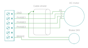
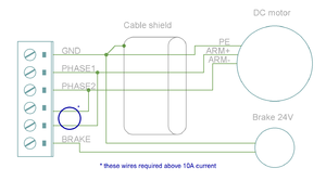
| Line 68: | Line 69: | ||
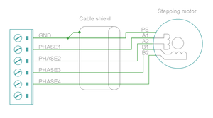
File:Ionicube mot step.png|Wiring of two phase stepping motor. Brake can be fitted like in the other examples. Also 6 and 8 wire motors can be wired (the two drive coils connect always to the same PHASE outputs). | File:Ionicube mot step.png|Wiring of two phase stepping motor. Brake can be fitted like in the other examples. Also 6 and 8 wire motors can be wired (the two drive coils connect always to the same PHASE outputs). | ||
</gallery> | </gallery> | ||
| + | {{tip|An easy way to verify correctness of two phase '''stepper''' connection: unplug the 6 pin connector and then measure resistance between phases 1-2 and 3-4. Multimeter should show the same resistance for both cases (typically 0.1 - 5 ohms). Also when measuring between phases 1-3, 1-4, 2-3 and 2-4, the multimeter should indicate open circuit.}} | ||
===X6 and X8 pinout=== | ===X6 and X8 pinout=== | ||
X6 and X8 are the [[feedback devices|feedback device]] connectors of motors | X6 and X8 are the [[feedback devices|feedback device]] connectors of motors | ||
| − | { | + | {{EncoderPinoutD15}} |
| − | | | + | {{info|Especially with long encoder cables, it might be necessary to add encoder line termination resistors, see [[Terminating differential encoder lines]].}} |
| − | + | ||
| − | + | ||
| − | + | ||
| − | + | ||
| − | + | ||
| − | + | ||
| − | + | ||
| − | + | ||
| − | + | ||
| − | + | ||
| − | + | ||
| − | + | ||
| − | + | ||
| − | + | ||
| − | + | ||
| − | + | ||
| − | + | ||
| − | + | ||
| − | + | ||
| − | + | ||
| − | + | ||
| − | + | ||
| − | + | ||
| − | + | ||
| − | + | ||
| − | + | ||
| − | + | ||
| − | + | ||
| − | + | ||
| − | + | ||
| − | + | ||
| − | + | ||
| − | + | ||
| − | + | ||
====Examples of feedback device and switch wiring==== | ====Examples of feedback device and switch wiring==== | ||
<gallery widths="180px" heights="180px"> | <gallery widths="180px" heights="180px"> | ||
| Line 135: | Line 103: | ||
! Pin number !! Signal name !! Usage | ! Pin number !! Signal name !! Usage | ||
|- | |- | ||
| − | | 1 ||class="powpin"| GND|| Ground | + | | 1 || class="powpin" | GND|| Ground |
|- | |- | ||
| − | | 2|| class="powpin"|24V || 24V logic supply | + | | 2|| class="powpin" |24V || 24V logic supply |
|- | |- | ||
| − | | 3|| class="inpin"|STO || Safe torque off input (this pin also available in X1, as defined in [[SimpleMotion V2 port]] | + | | 3|| class="inpin" |STO || Safe torque off input (this pin also available in X1, as defined in [[SimpleMotion V2 port]] |
|- | |- | ||
| − | | 4||class="outpin"| VFD || 0-12V analog output where voltage level is proportional to [[PWM]] duty cycle on pin PWM on X4. PWM frequency must be between 100 and 10000 Hz. | + | | 4|| class="outpin" | VFD || 0-12V analog output where voltage level is proportional to [[PWM]] duty cycle on pin PWM on X4. PWM frequency must be between 100 and 10000 Hz. |
|- | |- | ||
| − | | 5|| class="outpin"|RL1 || Relay coil driver output 1. When RLIN1 on X4 is logic high, RL1 is pulled to GND by an open collector circuit. When RLIN1 is low, RL1 is floating (max 24V). | + | | 5|| class="outpin" |RL1 || Relay coil driver output 1. When RLIN1 on X4 is logic high, RL1 is pulled to GND by an open collector circuit. When RLIN1 is low, RL1 is floating (max 24V). When connecting a relay that has 24VDC coil between RL1 and supplied 24V, no external free-wheeling diode is needed. Output current rating is max 500 mA. |
|- | |- | ||
| − | | 6|| class="outpin"|RL2 || Relay coil driver output 2. When RLIN2 on X4 is logic high, RL2 is pulled to GND by an open collector circuit. When RLIN1 is low, RL2 is floating (max 24V). | + | | 6|| class="outpin" |RL2 || Relay coil driver output 2. When RLIN2 on X4 is logic high, RL2 is pulled to GND by an open collector circuit. When RLIN1 is low, RL2 is floating (max 24V). When connecting a relay that has 24VDC coil between RL2 and supplied 24V, no external free-wheeling diode is needed. Output current rating is max 500 mA. |
|} | |} | ||
| + | |||
===X3 pinout=== | ===X3 pinout=== | ||
X3 is two pin wire terminal for [[HV DC bus]] supply. | X3 is two pin wire terminal for [[HV DC bus]] supply. | ||
| Line 153: | Line 122: | ||
! Pin number !! Signal name !! Usage | ! Pin number !! Signal name !! Usage | ||
|- | |- | ||
| − | | 1 ||class="powpin"| GND|| Ground | + | | 1 || class="powpin" | GND|| Ground |
|- | |- | ||
| − | | 2|| class="powpin"|HV+ || Motor power supply, [[HV DC bus]] (see IONI drive voltage range spec) | + | | 2|| class="powpin" |HV+ || Motor power supply, [[HV DC bus]] (see IONI drive voltage range spec) |
|} | |} | ||
| + | See also: | ||
| + | *[[IONI power supply schemes]] | ||
| + | *[[Estimating power need of motor drive system]] | ||
| + | {{info|If using switching power supply (SMPS) as motor power supply, external rectifier diodes are needed to protect the power supplies. See See [[IONI power supply schemes]].}} | ||
===X4 pinout=== | ===X4 pinout=== | ||
| Line 162: | Line 135: | ||
{| class="wikitable" | {| class="wikitable" | ||
! Pin number in header!!Pin number in D25 cable!!Signal name!!Typical usage | ! Pin number in header!!Pin number in D25 cable!!Signal name!!Typical usage | ||
| − | |rowspan=14 class="tableseparator"| | + | | rowspan="14" class="tableseparator" | |
!Pin number in header!!Pin number in D25 cable!!Signal name!!Typical usage | !Pin number in header!!Pin number in D25 cable!!Signal name!!Typical usage | ||
|- | |- | ||
| − | | 1||1||class="inpin"|ENABLE |||Enable all axis (with or without chargepump)||2||14||class="inpin"|PWM||[[PWM]] input for VFD analog output | + | | 1||1|| class="inpin" |ENABLE |||Enable all axis (with or without chargepump)||2||14|| class="inpin" |PWM||[[PWM]] input for VFD analog output |
|- | |- | ||
| − | | 3||2||class="inpin"|HSIN1_X|| | + | | 3||2|| class="inpin" |HSIN1_X||Pulse/step input X||4||15|| class="outpin" |GPO4_A||Limit switch output A |
|- | |- | ||
| − | | 5||3||class="inpin"|HSIN2_X|| | + | | 5||3|| class="inpin" |HSIN2_X||Direction input X||6||16|| class="inpin" |RLIN1||Controls RL1 state |
|- | |- | ||
| − | | 7||4||class="inpin"|HSIN1_Y|| | + | | 7||4|| class="inpin" |HSIN1_Y||Pulse/step input Y||8||17|| class="inpin" |RLIN2||Controls RL2 state |
|- | |- | ||
| − | | 9||5||class="inpin"|HSIN2_Y|| | + | | 9||5|| class="inpin" |HSIN2_Y||Direction input Y||10||18|| class="powpin" |GND|| rowspan="8" |Ground |
|- | |- | ||
| − | | 11||6||class="inpin"|HSIN1_Z|| | + | | 11||6|| class="inpin" |HSIN1_Z||Pulse/step input Z||12||19|| class="powpin" |GND |
|- | |- | ||
| − | | 13||7||class="inpin"|HSIN2_Z|| | + | | 13||7|| class="inpin" |HSIN2_Z||Direction input Z||14||20|| class="powpin" |GND |
|- | |- | ||
| − | | 15||8||class="inpin"|HSIN1_A|| | + | | 15||8|| class="inpin" |HSIN1_A||Pulse/step input A||16||21|| class="powpin" |GND |
|- | |- | ||
| − | | 17||9||class="inpin"|HSIN2_A|| | + | | 17||9|| class="inpin" |HSIN2_A||Direction input A||18||22|| class="powpin" |GND |
|- | |- | ||
| − | | 19||10||class="outpin"|STOP_OUT||Fault on any axis or E-stop (active low)||20||23||class="powpin"|GND | + | | 19||10|| class="outpin" |STOP_OUT||Fault on any axis or E-stop (active low). Note: this is IONI's GPO3 signals connected in parallel between all axis / [https://en.wikipedia.org/wiki/Wired_logic_connection wired-or configuration].||20||23|| class="powpin" |GND |
|- | |- | ||
| − | | 21||11||class="outpin"|GPO4_X||Limit switch output X||22||24||class="powpin"|GND | + | | 21||11|| class="outpin" |GPO4_X||Limit switch output X||22||24|| class="powpin" |GND |
|- | |- | ||
| − | | 23||12||class="outpin"|GPO4_Y||Limit switch output Y||24||25||class="powpin"|GND | + | | 23||12|| class="outpin" |GPO4_Y||Limit switch output Y||24||25|| class="powpin" |GND |
|- | |- | ||
| − | | 25||13||class="outpin"|GPO4_Z||Limit switch output Z||26||N/A||Not connected|| | + | | 25||13|| class="outpin" |GPO4_Z||Limit switch output Z||26||N/A||Not connected|| |
| + | |- | ||
| + | | Pin layout || colspan=8 | [[File:26_pin_header_pinout.png|frameless|500x500px]] | ||
|} | |} | ||
| + | {{damage|Connect only to 3.3V or 5V logic circuits go any GPI, GPO and HSIN pins. Most of X4 & X5 pins are directly routed to IONI drive pins and [[IONI connector pinout|IONI electrical ratings]] apply.}} | ||
| − | {{ | + | ====Alternative setpoint signals==== |
| + | {{Template:IONI setpoint signals}} | ||
===X5 pinout=== | ===X5 pinout=== | ||
| Line 198: | Line 175: | ||
{| class="wikitable" | {| class="wikitable" | ||
! Pin number in header!!Pin number in D25 cable!!Signal name!!Typical usage | ! Pin number in header!!Pin number in D25 cable!!Signal name!!Typical usage | ||
| − | |rowspan=14 class="tableseparator"| | + | | rowspan="14" class="tableseparator" | |
!Pin number in header!!Pin number in D25 cable!!Signal name!!Typical usage | !Pin number in header!!Pin number in D25 cable!!Signal name!!Typical usage | ||
|- | |- | ||
| − | | 1||1||class="powpin"|GND||||2||14||class="powpin"|+5V_OUT||5V supply from IONICUBE ^2 | + | | 1||1|| class="powpin" |GND||||2||14|| class="powpin" |+5V_OUT||5V supply from IONICUBE ^2 |
|- | |- | ||
| − | | 3||2||class="inpin"|ANAIN-_X||+/-10V analog input X||4||15||class="inpin"|ANAIN+_X||+/-10V analog input X | + | | 3||2|| class="inpin" |ANAIN-_X||+/-10V analog input X||4||15|| class="inpin" |ANAIN+_X||+/-10V analog input X |
|- | |- | ||
| − | | 5||3||class="inpin"|ANAIN-_Y||+/-10V analog input Y||6||16||class="inpin"|ANAIN+_Y||+/-10V analog input Y | + | | 5||3|| class="inpin" |ANAIN-_Y||+/-10V analog input Y||6||16|| class="inpin" |ANAIN+_Y||+/-10V analog input Y |
|- | |- | ||
| − | | 7||4||class="inpin"|ANAIN-_Z||+/-10V analog input Z||8||17||class="inpin"|ANAIN+_Z||+/-10V analog input Z | + | | 7||4|| class="inpin" |ANAIN-_Z||+/-10V analog input Z||8||17|| class="inpin" |ANAIN+_Z||+/-10V analog input Z |
|- | |- | ||
| − | | 9||5||class="inpin"|ANAIN-_A||+/-10V analog input A||10||18||class="inpin"|ANAIN+_A||+/-10V analog input A | + | | 9||5|| class="inpin" |ANAIN-_A||+/-10V analog input A||10||18|| class="inpin" |ANAIN+_A||+/-10V analog input A |
|- | |- | ||
| − | | 11||6||class="outpin"|GPO1_X||rowspan=8|For pin function, refer to [[IONI connector pinout]] ||12||19||class="inpin"|GPI4_X||rowspan=8|For pin function, refer to [[IONI connector pinout]] | + | | 11||6|| class="outpin" |GPO1_X|| rowspan="8" |For pin function, refer to [[IONI connector pinout]] ||12||19|| class="inpin" |GPI4_X|| rowspan="8" |For pin function, refer to [[IONI connector pinout]] |
|- | |- | ||
| − | | 13||7||class="outpin"|GPO1_Y ||14||20||class="inpin"|GPI4_Y | + | | 13||7|| class="outpin" |GPO1_Y ||14||20|| class="inpin" |GPI4_Y |
|- | |- | ||
| − | | 15||8||class="outpin"|GPO1_Z ||16||21||class="inpin"|GPI4_Z | + | | 15||8|| class="outpin" |GPO1_Z ||16||21|| class="inpin" |GPI4_Z |
|- | |- | ||
| − | | 17||9||class="outpin"|GPO1_A ||18||22||class="inpin"|GPI4_A | + | | 17||9|| class="outpin" |GPO1_A ||18||22|| class="inpin" |GPI4_A |
|- | |- | ||
| − | | 19||10||class="outpin"|GPO5_X ||20||23||class="inpin"|GPI5_X | + | | 19||10|| class="outpin" |GPO5_X ||20||23|| class="inpin" |GPI5_X |
|- | |- | ||
| − | | 21||11||class="outpin"|GPO5_Y ||22||24||class="inpin"|GPI5_Y | + | | 21||11|| class="outpin" |GPO5_Y ||22||24|| class="inpin" |GPI5_Y |
|- | |- | ||
| − | | 23||12||class="outpin"|GPO5_Z ||24||25||class="inpin"|GPI5_Z | + | | 23||12|| class="outpin" |GPO5_Z ||24||25|| class="inpin" |GPI5_Z |
|- | |- | ||
| − | | 25||13||class="outpin"|GPO5_A ||26||N/A||class="inpin"|GPI5_A | + | | 25||13|| class="outpin" |GPO5_A ||26||N/A|| class="inpin" |GPI5_A |
| + | |- | ||
| + | | Pin layout || colspan=8 | [[File:26_pin_header_pinout.png|frameless|500x500px]] | ||
|} | |} | ||
| − | <gallery widths="180px" heights="180px"> | + | == Application example == |
| + | Follwing image shows typical installation schemes for pulse/direction controlled systems, typically found in PC CNC applications.<gallery widths="180px" heights="180px"> | ||
File:ionicube stepdir.png|A typical connection with parallel port style CNC controller such as [[Mach3]]/[[Mach4]]/[[LinuxCNC]]. A 26 pin ribbon cable may be directly connected to PC parallel port or to equivalent pinout step/dir generator such as [[SmoothStepper]]. | File:ionicube stepdir.png|A typical connection with parallel port style CNC controller such as [[Mach3]]/[[Mach4]]/[[LinuxCNC]]. A 26 pin ribbon cable may be directly connected to PC parallel port or to equivalent pinout step/dir generator such as [[SmoothStepper]]. | ||
</gallery> | </gallery> | ||
| − | [[ | + | [[Category:IONI_user_guide]] |
| − | [[ | + | [[Category:IONICUBE]] |
Latest revision as of 12:35, 11 December 2017
IONICUBE connectors[edit | edit source]
- X1
- Dual port RJ45 connector with SimpleMotion V2 interface. For pinout, seeSimpleMotion V2 port.
- X2
- 6 pin wire terminal for logic voltage supply, Safe torque off input, analog output and relay driver outputs.
- X3
- Two pin wire terminal for HV DC bus supply.
- X4
- Main control and setpoint signal port consisting Enable input signal, Fault output signal, pulse and direction/quadrature/PWM setpoint inputs and digital outputs for home switch status. X4 is directly wired to conform most common parallel port style pulse & direction CNC controllers.
- X5
- Second control and setpoint signal port. This port consists analog setpoint signal inputs and additional digital I/O.
- X6
- These are the feedback device connector for X (lower) and Y (upper) axis motors
- X7
- These are the power and holding brake output connector for X (lower) and Y (upper) axis motors
- X8
- These are the feedback device connector for Z (lower) and A (upper) axis motors
- X9
- These are the power and holding brake output connector for Z (lower) and A (upper) axis motors
- X10
- A connector for an optional external regenerative resistor. IONICUBE has on-board regenerative resistor that is sufficient for most installations.
- IONI_X, IONI_Y, IONI_Z, IONI_A
- Card-edge connectors for IONI drives
| Before inserting or removing IONI drives from IONICUBE, remove all power from it and discharge it's capacitors. To discharge remaining energy (~voltage) from capacitors, short circuit GND to HV+ by a conductor and measure that there is no DC voltage left between GND and HV+ terminals. Even few volts left to HV DC bus is known to cause permanent damage to IONICUBE when drives are plugged. |
Front side connectors[edit | edit source]
Front side connectors consist X6, X7, X8 and X9. These connectors are the interface towards motors (motor power and feedback devices).

Names of power and feedback ports. I.e. X9A means upper floor connector of X9 and X9B the lower floor of X9. View from plug side of the board.
Legend[edit | edit source]
| Color |
|---|
| Supply pin |
| Input pin |
| Output pin |
X7 and X9 pinout[edit | edit source]
These are the power output and holding brake output connector for motors
| Pin number | Signal name | AC/BLDC motor | Brush DC motor | Stepping motor |
|---|---|---|---|---|
| 1 | GND | Ground for cable shield and an optional motor holding brake coil | ||
| 2 | PHASE1 | U (some motors R) | Armature + | Coil A.1 |
| 3 | PHASE2 | V (some motors S) | Armature - | Coil A.2 |
| 4 | PHASE3 | W (some motors T) | Armature - | Coil B.1 |
| 5 | PHASE4 | Not connected | Armature + | Coil B.2 |
| 6 | BRAKE | Optional 24V motor holding brake coil | ||
Motor & brake wiring schematics[edit | edit source]
| An easy way to verify correctness of two phase stepper connection: unplug the 6 pin connector and then measure resistance between phases 1-2 and 3-4. Multimeter should show the same resistance for both cases (typically 0.1 - 5 ohms). Also when measuring between phases 1-3, 1-4, 2-3 and 2-4, the multimeter should indicate open circuit. |
X6 and X8 pinout[edit | edit source]
X6 and X8 are the feedback device connectors of motors
| Pin # | Pin name | Electrical type (in most feedback device modes) | Quadrature encoder | SinCos encoder | BiSS-C encoder | SSI encoder | AMS SSI encoder |
|---|---|---|---|---|---|---|---|
| Shell | GND | Earth/case | |||||
| 1 | HALL_W | Hall sensor digital input, phase W | - | - | - | ||
| 2 | HALL_V | Hall sensor digital input, phase V | - | - | - | ||
| 3 | HALL_U | Hall sensor digital input, phase U | - | - | - | ||
| 4 | GND | Encoder supply ground | |||||
| 5 | B- | Differential input B- | Channel B- | SinCos input B- | - | - | - |
| 6 | B+ | Differential input B+ | Channel B+ | SinCos input B+ | - | - | - |
| 7 | A- | Differential input A- | Channel A- | SinCos input A- | - | - | - |
| 8 | A+ | Differential input A+ | Channel A+ | SinCos input A+ | - | - | - |
| 9 | 5V_OUT | Encoder supply 5V output | |||||
| 10 | GND | Encoder supply ground | |||||
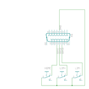
| 11 | GPI3 | Axis negative direction end limit switch (optional). Normally closed (NC) switch is highly recommended for safety reasons. Connect it between this pin and GND pin. Normally open (NO) switch can be used, and the switch polarity can be changed with Limit switch polarityLSP. |
Clock/MA- | Clock- | CLK | ||
| 12 | GPI2 | Axis positive direction end limit switch (optional).Normally closed (NC) switch is highly recommended for safety reasons. Connect it between this pin and GND pin. Normally open (NO) switch can be used, and the switch polarity can be changed with Limit switch polarityLSP. |
Clock/MA+ | Clock+ | CSn | ||
| 13 | GPI1 | Axis home switch switch (optional). Normally closed (NC) switch is highly recommended for safety reasons. Connect it between this pin and GND pin. Normally open (NO) switch can be used, and the switch polarity can be changed with Home switch or hard stop search direction (Home switch polarity)HMS. |
DO | ||||
| 14 | C- | Differential input C- | Index channel Z- | Index channel Z+ | Data/SLO- | Data- | - |
| 15 | C+ | Differential input C+ | Index channel Z+ | Index channel Z+ | Data/SLO+ | Data+ | - |
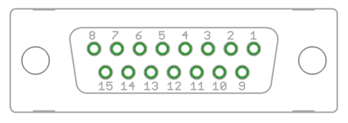
| Pin layout | Female D-sub 15 connector as it appears from outside of drive. Note: counterpart (male) connector has mirrored pin layout if viewed from pin side, and same layout if viewed from soldering side. | ||||||
| Especially with long encoder cables, it might be necessary to add encoder line termination resistors, see Terminating differential encoder lines. |
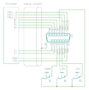
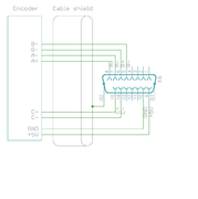
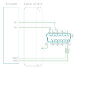
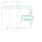
Examples of feedback device and switch wiring[edit | edit source]
| In case of single-ended encoder, connect encoder's A, B, Z only to drive's A+, B+ and C+ and leave drive's A-, B- and C- unconnected. |
| With differential Hall sensor (which provides U+, U-, V+, V-, W+ and W-, connect only sensor's U+, V+ and W+ to drive's HALL_U/V/W. |
| Never connect sensor negative outputs (A-/B-/C-/U-/V-/W-) to GND. Connect them to drive's A-/B-/C- or leave unconnected. |
| Feedback devices with differential signaling may use varying naming schemes of signal pairs. For example differential signal X (which contains two electrical wires) may be denoted as: X+ and X-, or X and \X or X and X. In this Wiki we mark them X+ and X-. Some Fanuc encoders have quadrature signals named as PCA, /PCA, PCB, /PCB, PCZ and /PCZ which are equivalent to A, B and Z signal pairs. |
Back side connectors[edit | edit source]
| Never connect an Ethernet to X1. While it uses similar connector and cabling, it is electrically incompatible with Ethernet. Devices may be permanently damaged by mixing Ethernet and SimpleMotion V2. |
| Do now wire SimpleMotion V2 ports with crossover RJ45 cables (see details). Always use straight/non-crossover patch cables. If unsure about what is the type of your RJ45 cable, don't use it. |
X2 pinout[edit | edit source]
X2 is 6 pin wire terminal for logic voltage supply, Safe torque off input, analog output and relay driver outputs.
| Pin number | Signal name | Usage |
|---|---|---|
| 1 | GND | Ground |
| 2 | 24V | 24V logic supply |
| 3 | STO | Safe torque off input (this pin also available in X1, as defined in SimpleMotion V2 port |
| 4 | VFD | 0-12V analog output where voltage level is proportional to PWM duty cycle on pin PWM on X4. PWM frequency must be between 100 and 10000 Hz. |
| 5 | RL1 | Relay coil driver output 1. When RLIN1 on X4 is logic high, RL1 is pulled to GND by an open collector circuit. When RLIN1 is low, RL1 is floating (max 24V). When connecting a relay that has 24VDC coil between RL1 and supplied 24V, no external free-wheeling diode is needed. Output current rating is max 500 mA. |
| 6 | RL2 | Relay coil driver output 2. When RLIN2 on X4 is logic high, RL2 is pulled to GND by an open collector circuit. When RLIN1 is low, RL2 is floating (max 24V). When connecting a relay that has 24VDC coil between RL2 and supplied 24V, no external free-wheeling diode is needed. Output current rating is max 500 mA. |
X3 pinout[edit | edit source]
X3 is two pin wire terminal for HV DC bus supply.
| Pin number | Signal name | Usage |
|---|---|---|
| 1 | GND | Ground |
| 2 | HV+ | Motor power supply, HV DC bus (see IONI drive voltage range spec) |
See also:
| If using switching power supply (SMPS) as motor power supply, external rectifier diodes are needed to protect the power supplies. See See IONI power supply schemes. |
X4 pinout[edit | edit source]
X4 is main control and setpoint signal port consisting Enable input signal, Fault output signal, pulse and direction/quadrature/PWM setpoint inputs and digital outputs for home switch status. X4 is directly wired to conform most common parallel port style pulse & direction CNC controllers.
| Pin number in header | Pin number in D25 cable | Signal name | Typical usage | Pin number in header | Pin number in D25 cable | Signal name | Typical usage | |
|---|---|---|---|---|---|---|---|---|
| 1 | 1 | ENABLE | Enable all axis (with or without chargepump) | 2 | 14 | PWM | PWM input for VFD analog output | |
| 3 | 2 | HSIN1_X | Pulse/step input X | 4 | 15 | GPO4_A | Limit switch output A | |
| 5 | 3 | HSIN2_X | Direction input X | 6 | 16 | RLIN1 | Controls RL1 state | |
| 7 | 4 | HSIN1_Y | Pulse/step input Y | 8 | 17 | RLIN2 | Controls RL2 state | |
| 9 | 5 | HSIN2_Y | Direction input Y | 10 | 18 | GND | Ground | |
| 11 | 6 | HSIN1_Z | Pulse/step input Z | 12 | 19 | GND | ||
| 13 | 7 | HSIN2_Z | Direction input Z | 14 | 20 | GND | ||
| 15 | 8 | HSIN1_A | Pulse/step input A | 16 | 21 | GND | ||
| 17 | 9 | HSIN2_A | Direction input A | 18 | 22 | GND | ||
| 19 | 10 | STOP_OUT | Fault on any axis or E-stop (active low). Note: this is IONI's GPO3 signals connected in parallel between all axis / wired-or configuration. | 20 | 23 | GND | ||
| 21 | 11 | GPO4_X | Limit switch output X | 22 | 24 | GND | ||
| 23 | 12 | GPO4_Y | Limit switch output Y | 24 | 25 | GND | ||
| 25 | 13 | GPO4_Z | Limit switch output Z | 26 | N/A | Not connected | ||
| Pin layout | 
| |||||||
| Connect only to 3.3V or 5V logic circuits go any GPI, GPO and HSIN pins. Most of X4 & X5 pins are directly routed to IONI drive pins and IONI electrical ratings apply. |
Alternative setpoint signals[edit | edit source]
Setpoint mode is selected by software with parameter Setpoint inputCRI and behavior is affected by parameters Setpoint smoothingCIS, Setpoint multiplierMUL, Setpoint dividerDIV, Setpoint offset nullingCAO and Enable direction inputCED.
| Drive listens setpoint commands also always through SimpleMotion V2 interface regardess of Setpoint inputCRI paramter setting. |
| Signal name | Function | Used for | Remarks |
|---|---|---|---|
| HSIN1 | High speed digital input 1 | Depending on setpoint mode, can be either:
| |
| HSIN2 | High speed digital input 2 | Depending on setpoint mode, can be either:
| |
| ANAIN- | Differential analog negative input | Used for analog setpoint mode | Setpoint voltage is the voltage difference between ANAIN+ and ANAIN- |
| ANAIN+ | Differential analog positive input | Used for analog setpoint mode |
X5 pinout[edit | edit source]
X5 is a second control and setpoint signal port in addition to X4. This port consists analog setpoint signal inputs and additional digital I/O.
| Pin number in header | Pin number in D25 cable | Signal name | Typical usage | Pin number in header | Pin number in D25 cable | Signal name | Typical usage | |
|---|---|---|---|---|---|---|---|---|
| 1 | 1 | GND | 2 | 14 | +5V_OUT | 5V supply from IONICUBE ^2 | ||
| 3 | 2 | ANAIN-_X | +/-10V analog input X | 4 | 15 | ANAIN+_X | +/-10V analog input X | |
| 5 | 3 | ANAIN-_Y | +/-10V analog input Y | 6 | 16 | ANAIN+_Y | +/-10V analog input Y | |
| 7 | 4 | ANAIN-_Z | +/-10V analog input Z | 8 | 17 | ANAIN+_Z | +/-10V analog input Z | |
| 9 | 5 | ANAIN-_A | +/-10V analog input A | 10 | 18 | ANAIN+_A | +/-10V analog input A | |
| 11 | 6 | GPO1_X | For pin function, refer to IONI connector pinout | 12 | 19 | GPI4_X | For pin function, refer to IONI connector pinout | |
| 13 | 7 | GPO1_Y | 14 | 20 | GPI4_Y | |||
| 15 | 8 | GPO1_Z | 16 | 21 | GPI4_Z | |||
| 17 | 9 | GPO1_A | 18 | 22 | GPI4_A | |||
| 19 | 10 | GPO5_X | 20 | 23 | GPI5_X | |||
| 21 | 11 | GPO5_Y | 22 | 24 | GPI5_Y | |||
| 23 | 12 | GPO5_Z | 24 | 25 | GPI5_Z | |||
| 25 | 13 | GPO5_A | 26 | N/A | GPI5_A | |||
| Pin layout | 
| |||||||
Application example[edit | edit source]
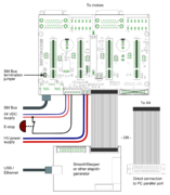
Follwing image shows typical installation schemes for pulse/direction controlled systems, typically found in PC CNC applications.A typical connection with parallel port style CNC controller such as Mach3/Mach4/LinuxCNC. A 26 pin ribbon cable may be directly connected to PC parallel port or to equivalent pinout step/dir generator such as SmoothStepper.
