Difference between revisions of "Intensify Nx50 setup guide"
| [checked revision] | [checked revision] |
(→Connecting parallel) |
(→Digital signals: update logic high voltage from 3.0 to 4.5v min) |
||
| Line 71: | Line 71: | ||
| Logic LOW|| -0.3 .. 0.6V | | Logic LOW|| -0.3 .. 0.6V | ||
|- | |- | ||
| − | | Logic HIGH|| | + | | Logic HIGH|| 4.5 - 26 V |
|} | |} | ||
Revision as of 10:36, 11 May 2016

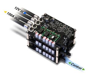
This is the intallation & user guide for the Intensify Nx50 laser diode driver. Read it through before operating the device.
In case of any questions, please don't hesitate to contact us.
| Pre-production version of Nx50 setup guide can be found [here]. Please note that some I/O signal characteristics and pin out has changed. |
Contents
Physical installation and cooling
Nx50 should be mounted inside an enclosure by using spacer feet attached to the four corner holes.
Nx50 has low power losses due to highly efficient multiphase switching converter technology. Power loss can be calculated by using the offered efficiency data as setpont.
In most cases Nx50 is sufficiently cooled with natural convection. This is best achieved by mounting boards vertically and leaving at least 25 mm free air space around both sides.
However, if natural convection does not offer sufficient cooling (i.e. if peak surface temperature is near or exceeds 100°C), then forced convection is necessary. This can be achieved by placing a fan or blower on the side of PCB so that air flow passes along board surface.
Wiring
Before wiring, review Nx50 electrical specifications.
J1 connector
J1 connector is the user side I/O of the driver. This connector contains the control and feedback signals. All signal lines of the port are ESD protected by dedicated suppressors.
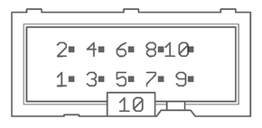
Mating connector type is a 10 pin flat ribbon cable connector with 0.1"/2.54 mm pin pitch and a polarity key. See spec sheet of compatible connector here.
J1 pin out
| Pin # | Signal name | Direction | Signal description | Impedance vs GND |
|---|---|---|---|---|
| 1 | PULSE | In | Pulse control:
|
10 kOhm |
| 2 | GND | I/O and power ground | I/O and Analog ground | 0 Ohm |
| 3 | IMON | Out | Current monitor 0-10 V analog output | 1 kOhm |
| 4 | GND | I/O and power ground | I/O and Analog ground | 0 Ohm |
| 5 | VMON | Out | Voltage monitor 1:1 analog output | 1 kOhm |
| 6 | GND | I/O and power ground | 0 Ohm | |
| 7 | ISET+ | In | Current setpoint 0-10 V positive input (differential) | 51 kOhm |
| 8 | ISET- | In | Current setpoint 0-10 V negateive input (differential) | 51 kOhm |
| 9 | ENABLE | In | LDD enable:
|
6.6 kOhm |
| 10 | GND | I/O and power ground | I/O and Analog ground | 0 Ohm |
Impedances
When driving an J1 input pin, the source impedance of controller should be significantly lower than input impedance of the corresponding pin. I.e. if input impedance is 51 kOhm, then recommended source impedance is less than 5 kOhm max, preferrably 0.5 kOhm. Lower source impedance yields lower voltage drop error.
Also when an output of J1 is connected to the input of controller, the controller input impedance should be significantly higher than J1 pin impedance. I.e. when connecting VMON (1 kOhm) to analog input or ADC, the controller input impedance should be at least 10 kOhm. However all outputs are short circuit proof and input impedance recommendation affects only monitor accuracy.
See impedance column of pin out table
Digital signals
All digital signals (PULSE & ENABLE) are referenced to GND and applicable voltage levels are:
| State | Voltage range |
|---|---|
| Logic LOW | -0.3 .. 0.6V |
| Logic HIGH | 4.5 - 26 V |
Analog signals
Analog input signal support differential signaling to cancel noise and ground loop induced error. These are designed to be compatible with another differential source as well as single ended systems. The differential signals allow up to +/- 1.5V difference on ground reference potentials between Nx50 and controller without losing accuracy.
Connection to differential 0-10V analog I/O:
| Controller | J1 signal |
|---|---|
| Analog in 1 + | IMON |
| Analog in 1 - | GND |
| Analog in 2 + | VMON |
| Analog in 2 - | GND |
| Analog out 1 + | ISET+ |
| Analog out 1 - | ISET- |
| Ground | GND |
Connecting to single ended 0-10V analog I/O. Assuming that I/O is referenced to Ground.
| Controller | J1 signal |
|---|---|
| Analog in 1 | IMON |
| Analog in 2 | VMON |
| Analog out 1 | ISET+ |
| Ground | ISET- |
| Ground | GND |
Power
A regulated 12VDC power supply should be connected to hole terminals labeled GND and +12V. Required power is nearly directly proportional to output power plus losses.
For example outputting 40A to 2.0V diode equals output power of 80W. With losses the needed power is about 85-90W which equals 7.0-7.5A @ 12V.
Laser diode
Laser diode is connected to hole terminals labeled O+ and O-. O+ goes to LD anode and O- to cathode.
Connecting parallel
Nx50 boards may be connected parallel to increase output current range simply by connecting all power and I/O lines parallel pin-by-pin basis.
This can be achieved by stacking them by using metallic standoffs to form conductive path between O+, O-, GND, and +12V terminals. Use M4, M5, 10-24, 8-36, or #8 threaded standoffs with minimum height of 16 mm / 0.63".
J1 connector may be paralleled by inserting multiple 10 pin IDC connectors to the single ribbon cable. By this method all J1 pins are properly connected parallel pin-to-pin basis.
CMD connector output signals in parallel mode
When mutliple boards are wired parallel, the output of current and voltage monitor pins will be the average of individual driver board values.
I.e. if we have three Nx50 in parallel with the setpoint set of 10V (which normally outputs 150A current), then current monitor output would also give 10V. If one of boards is in fault state (overtemperature etc), then output current would be only 100A (two boards driving, one inactive). In such condition the current monitor output would be 6.67V (the average of 10V, 10V and 0V).
Usage
The device starts operating instantly after powered and and proper signals fed to J1 pins. No other initialization is needed. Sequence order of signals and power are not critical - device will not get harmed or produce erratic output regardless of start-up order.
CW usage
- Mandatory connections
- LD connected between O+/O-
- 12VDC supply connecter between +12V/GND
- J1 connector pins:
- GND connected to controller's ground reference:
- 0-10V current setpoint signal fed to ISET+/ISET-
- ENABLE set to HIGH or tied to GND
- Optional J1 connections
- IMON wired to analog input
- VMON wired to analog input
- PULSE set to HIGH or left open
Pulsed usage
For pulsed usage it is recommended to use PULSE input or modulate the ISET analog voltage. It is not recommended to set current to 0 during off-periods for to achieve faster pulse rise times and zero overshoot. Recommended bias current during off-periods is 2-10% of current setpoint.
- Mandatory connections
- LD connected between O+/O-
- 12VDC supply connecter between +12V/GND
- J1 connector pins:
- GND connected to controller's ground reference:
- 0-10V current setpoint signal fed to ISET+/ISET-
- ENABLE set to HIGH or tied to GNDA
- PULSE set pulse source. Logic LOW means 100% of set current and HIGH reduces output current to 3.5% (bias current to allow faster rise time)
- Optional J1 connections
- IMON wired to analog input
- VMON wired to analog input


