Difference between revisions of "IONICUBE connectors and pinouts"
From Granite Devices Knowledge Wiki
| [checked revision] | [checked revision] |
| Line 36: | Line 36: | ||
|} | |} | ||
===X3=== | ===X3=== | ||
| − | + | {| class="wikitable" | |
| + | |- | ||
| + | ! Pin number !! Signal name !! Usage | ||
| + | |- | ||
| + | | 1 ||class="powpin"| GND|| Ground | ||
| + | |- | ||
| + | | 2|| class="powpin"|HV+ || Motor power supply, [[HV DC bus]] (see IONI drive voltage range spec) | ||
| + | |} | ||
===X4=== | ===X4=== | ||
Revision as of 11:30, 21 March 2015

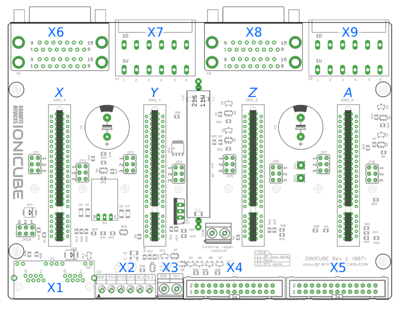
Names of power and feedback ports. I.e. X9A means upper floor connector of X9 and X9B the lower floor of X9.
Legend
| Color |
|---|
| Power pin |
| Input pin |
| Output pin |
X2
| Pin number | Signal name | Usage |
|---|---|---|
| 1 | GND | Ground |
| 2 | 24V | 24V logic supply |
| 3 | STO | Safe torque off input (this pin also available in X1, as defined in SimpleMotion V2 port |
| 4 | VFD | 0-12V analog output where voltage level is proportional to PWM duty cycle on pin PWM on X4. PWM frequency must be between 100 and 10000 Hz. |
| 5 | RL1 | Relay coil driver output 1. When RLIN1 on X4 is logic high, RL1 is pulled to GND by an open collector circuit. When RLIN1 is low, RL1 is floating (max 24V). |
| 6 | RL2 | Relay coil driver output 2. When RLIN2 on X4 is logic high, RL2 is pulled to GND by an open collector circuit. When RLIN1 is low, RL2 is floating (max 24V). |
X3
| Pin number | Signal name | Usage |
|---|---|---|
| 1 | GND | Ground |
| 2 | HV+ | Motor power supply, HV DC bus (see IONI drive voltage range spec) |
X4
| Pin number in header | Pin number in D25 cable | Signal name | Typical usage | Pin number in header | Pin number in D25 cable | Signal name | Typical usage | |
|---|---|---|---|---|---|---|---|---|
| 1 | 1 | ENABLE | Enable all axis (with or without chargepump) | 2 | 14 | PWM | PWM input for VFD analog output | |
| 3 | 2 | HSIN1_X | Direction input X | 4 | 15 | GPO4_A | Limit switch output A | |
| 5 | 3 | HSIN2_X | Pulse/step input X | 6 | 16 | RLIN1 | Controls RL1 state | |
| 7 | 4 | HSIN1_Y | Direction input Y | 8 | 17 | RLIN2 | Controls RL2 state | |
| 9 | 5 | HSIN2_Y | Pulse/step input Y | 10 | 18 | GND | Ground | |
| 11 | 6 | HSIN1_Z | Direction input Z | 12 | 19 | GND | ||
| 13 | 7 | HSIN2_Z | Pulse/step input A | 14 | 20 | GND | ||
| 15 | 8 | HSIN1_A | Direction input A | 16 | 21 | GND | ||
| 17 | 9 | HSIN2_A | Pulse/step input A | 18 | 22 | GND | ||
| 19 | 10 | STOP_OUT | Fault on any axis or E-stop (active low) | 20 | 23 | GND | ||
| 21 | 11 | GPO4_X | Limit switch output X | 22 | 24 | GND | ||
| 23 | 12 | GPO4_Y | Limit switch output Y | 24 | 25 | GND | ||
| 25 | 13 | GPO4_Z | Limit switch output Z | 26 | N/A | Not connected |
X5
| Pin number in header | Pin number in D25 cable | Signal name | Typical usage | Pin number in header | Pin number in D25 cable | Signal name | Typical usage | |
|---|---|---|---|---|---|---|---|---|
| 1 | 1 | GND | 2 | 14 | +5V_OUT | 5V supply from IONICUBE ^2 | ||
| 3 | 2 | ANAIN-_X | +/-10V analog input X | 4 | 15 | ANAIN+_X | +/-10V analog input X | |
| 5 | 3 | ANAIN-_Y | +/-10V analog input Y | 6 | 16 | ANAIN+_Y | +/-10V analog input Y | |
| 7 | 4 | ANAIN-_Z | +/-10V analog input Z | 8 | 17 | ANAIN+_Z | +/-10V analog input Z | |
| 9 | 5 | ANAIN-_A | +/-10V analog input A | 10 | 18 | ANAIN+_A | +/-10V analog input A | |
| 11 | 6 | GPO1_X | For pin function, refer to IONI connector pinout | 12 | 19 | GPI4_X | For pin function, refer to IONI connector pinout | |
| 13 | 7 | GPO1_Y | 14 | 20 | GPI4_Y | |||
| 15 | 8 | GPO1_Z | 16 | 21 | GPI4_Z | |||
| 17 | 9 | GPO1_A | 18 | 22 | GPI4_A | |||
| 19 | 10 | GPO5_X | 20 | 23 | GPI5_X | |||
| 21 | 11 | GPO5_Y | 22 | 24 | GPI5_Y | |||
| 23 | 12 | GPO5_Z | 24 | 25 | GPI5_Z | |||
| 25 | 13 | GPO5_A | 26 | N/A | GPI5_A
|


