Difference between revisions of "IONICUBE 1X connectors and pinouts"
| [checked revision] | [checked revision] |
(→X4 pinout) |
|||
| (24 intermediate revisions by 2 users not shown) | |||
| Line 14: | Line 14: | ||
==IONICUBE 1X connectors== | ==IONICUBE 1X connectors== | ||
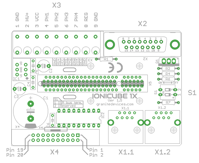
{{picturebox|Ionicube1x pinouts.png|caption=Connector layout and naming}} | {{picturebox|Ionicube1x pinouts.png|caption=Connector layout and naming}} | ||
| + | <br /> | ||
| + | {{picturebox|Ionicube1x wiring.png|caption=Wiring overview. R is regenerative resistor and E is encoder. In minimum working connection, wire 5V voltage to ENABLE and STO2 inputs into X4 pins (these two signals allow drive to be operated). Note: STO2 accepts voltage from 4.5 to 25 VDC but other digital inputs, such as ENABLE only between 2.7 to 5.5VDC.}} | ||
| + | {{info|If using switching power supply (SMPS) as motor power supply, external rectifier diodes are needed to protect the power supplies. See See [[IONI power supply schemes]].}} | ||
===Legend=== | ===Legend=== | ||
| Line 20: | Line 23: | ||
! Color | ! Color | ||
|- | |- | ||
| − | | class="powpin"|Supply pin | + | | class="powpin" |Supply pin |
|- | |- | ||
| − | | class="inpin"|Input pin | + | | class="inpin" |Input pin |
|- | |- | ||
| − | | class="outpin"|Output pin | + | | class="outpin" |Output pin |
|} | |} | ||
===X3 pinout=== | ===X3 pinout=== | ||
This is a wire terminal connector for power input and output | This is a wire terminal connector for power input and output | ||
| + | |||
{| class="wikitable" | {| class="wikitable" | ||
|- | |- | ||
! Pin number !! Signal name !! Usage | ! Pin number !! Signal name !! Usage | ||
|- | |- | ||
| − | | 1 ||class="powpin"| GND|| Ground | + | | 1 || class="powpin" | GND|| Ground |
|- | |- | ||
| − | | 2|| class="powpin"|HV+ || Motor power supply, [[HV DC bus]] (see IONI drive voltage range spec) | + | | 2|| class="powpin" |HV+ || Motor power supply, [[HV DC bus]] (see IONI drive voltage range spec) |
|- | |- | ||
| − | | 3|| class="powpin"|VCC || 24V logic supply | + | | 3|| class="powpin" |VCC || 24V logic supply |
|- | |- | ||
| − | | 4|| class="outpin"|PH1 (PHASE1) || Motor phase 1 | + | | 4|| class="outpin" |PH1 (PHASE1) || Motor phase 1 (see wiring table below) |
|- | |- | ||
| − | | 5|| class="outpin"|PH2 (PHASE2) || Motor phase 2 | + | | 5|| class="outpin" |PH2 (PHASE2) || Motor phase 2 (see wiring table below) |
|- | |- | ||
| − | | 6|| class="outpin"|PH3 (PHASE3) || Motor phase 3 | + | | 6|| class="outpin" |PH3 (PHASE3) || Motor phase 3 (see wiring table below) |
|- | |- | ||
| − | | 7|| class="outpin"|PH4 (PHASE4) || Motor phase 4 | + | | 7|| class="outpin" |PH4 (PHASE4) || Motor phase 4 (see wiring table below) |
|- | |- | ||
| − | | 8|| class="outpin"|REG || [[Regenerative resistor]] output | + | | 8|| class="outpin" |REG || [[Regenerative resistor]] output |
|- | |- | ||
| − | | 9 ||class="powpin"| GND|| Ground | + | | 9 || class="powpin" | GND|| Ground |
|} | |} | ||
| + | |||
| + | {| class="wikitable" | ||
| + | |- | ||
| + | ! Pin number !! Signal name !! AC/BLDC motor !! Brush DC motor !! Stepping motor | ||
| + | |- | ||
| + | | 1 || class="powpin" | GND|| colspan="3" | Ground for cable shield and an optional motor holding brake coil | ||
| + | |- | ||
| + | | 4|| class="outpin" |PHASE1 ||U (some motors R)||Armature +||Coil A.1 | ||
| + | |- | ||
| + | | 5|| class="outpin" |PHASE2 ||V (some motors S)||Armature -||Coil A.2 | ||
| + | |- | ||
| + | | 6|| class="outpin" |PHASE3 ||W (some motors T)||Armature -||Coil B.1 | ||
| + | |- | ||
| + | | 7|| class="outpin" |PHASE4 || Not connected||Armature +||Coil B.2 | ||
| + | |||
| + | |} | ||
| + | |||
====Motor & brake wiring schematics==== | ====Motor & brake wiring schematics==== | ||
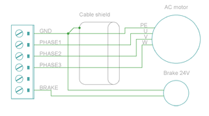
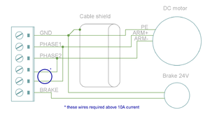
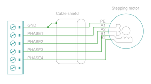
Note: the images below are drawn for [[IONICUBE]] 4 axis version. IONICUBE 1X wiring is equivalent except there is no brake output in the X3. Brake output pin is located in X4. | Note: the images below are drawn for [[IONICUBE]] 4 axis version. IONICUBE 1X wiring is equivalent except there is no brake output in the X3. Brake output pin is located in X4. | ||
| Line 57: | Line 78: | ||
File:Ionicube mot step.png|Wiring of two phase stepping motor. Brake can be fitted like in the other examples. Also 6 and 8 wire motors can be wired (the two drive coils connect always to the same PHASE outputs). | File:Ionicube mot step.png|Wiring of two phase stepping motor. Brake can be fitted like in the other examples. Also 6 and 8 wire motors can be wired (the two drive coils connect always to the same PHASE outputs). | ||
</gallery> | </gallery> | ||
| + | {{tip|An easy way to verify correctness of two phase '''stepper''' connection: unplug the 6 pin connector and then measure resistance between phases 1-2 and 3-4. Multimeter should show the same resistance for both cases (typically 0.1 - 5 ohms). Also when measuring between phases 1-3, 1-4, 2-3 and 2-4, the multimeter should indicate open circuit.}} | ||
| + | |||
| + | ====Regenerative resistor==== | ||
| + | [[Regenerative resistor]] is optional and may be connected between REG and HV+ terminals. The on board transistor is capable of carrying max 10 Amp current on regenerative resistor, so ''minimum'' allowed resistance can be calculated from: R<sub>min</sub>=HV<sub>voltage</sub>/10. I.e. with 48VDC HV supply, the minimum resistance is 48V/10A = 4.8 Ohms. Suggested resistor power capability is 20-100 W. | ||
| + | {{tip|When multiple IONICUBE 1X's are connected to a shared HV supply, then it is typically sufficient to have regenerative resistor only in one IONICUBE 1X as it will help to prevent voltage build-up in the HV supply line.}} | ||
===X2 pinout=== | ===X2 pinout=== | ||
X2 is the [[feedback devices|feedback device]] connector of motor | X2 is the [[feedback devices|feedback device]] connector of motor | ||
| − | { | + | {{EncoderPinoutD15}} |
| − | | | + | {{info|Especially with long encoder cables, it might be necessary to add encoder line termination resistors, see [[Terminating differential encoder lines]].}} |
| − | + | ||
| − | + | ||
| − | + | ||
| − | + | ||
| − | + | ||
| − | + | ||
| − | + | ||
| − | + | ||
| − | + | ||
| − | + | ||
| − | + | ||
| − | + | ||
| − | + | ||
| − | + | ||
| − | + | ||
| − | + | ||
| − | + | ||
| − | + | ||
| − | + | ||
| − | + | ||
| − | + | ||
| − | + | ||
| − | + | ||
| − | + | ||
| − | + | ||
| − | + | ||
| − | + | ||
| − | + | ||
| − | + | ||
| − | + | ||
| − | + | ||
| − | + | ||
| − | + | ||
| − | + | ||
====Examples of feedback device and switch wiring==== | ====Examples of feedback device and switch wiring==== | ||
<gallery widths="180px" heights="180px"> | <gallery widths="180px" heights="180px"> | ||
| Line 110: | Line 102: | ||
{{info|Never connect sensor negative outputs (A-/B-/C-/U-/V-/W-) to GND. Connect them to drive's A-/B-/C- or leave unconnected.}} | {{info|Never connect sensor negative outputs (A-/B-/C-/U-/V-/W-) to GND. Connect them to drive's A-/B-/C- or leave unconnected.}} | ||
{{tip|Feedback devices with [[differential signaling]] may use varying naming schemes of signal pairs. For example differential signal X (which contains two electrical wires) may be denoted as: X+ and X-, or X and \X or X and {{overline|X}}. In this Wiki we mark them X+ and X-. Some Fanuc encoders have quadrature signals named as PCA, /PCA, PCB, /PCB, PCZ and /PCZ which are equivalent to A, B and Z signal pairs.}} | {{tip|Feedback devices with [[differential signaling]] may use varying naming schemes of signal pairs. For example differential signal X (which contains two electrical wires) may be denoted as: X+ and X-, or X and \X or X and {{overline|X}}. In this Wiki we mark them X+ and X-. Some Fanuc encoders have quadrature signals named as PCA, /PCA, PCB, /PCB, PCZ and /PCZ which are equivalent to A, B and Z signal pairs.}} | ||
| − | |||
| − | |||
| − | |||
| − | |||
| − | |||
| − | |||
===X4 pinout=== | ===X4 pinout=== | ||
| Line 124: | Line 110: | ||
{| class="wikitable" | {| class="wikitable" | ||
! Pin number in header!!Signal name!!Typical usage | ! Pin number in header!!Signal name!!Typical usage | ||
| − | | | + | | class="tableseparator" rowspan="14" | |
!Signal name!!Typical usage | !Signal name!!Typical usage | ||
|- | |- | ||
| − | | 1||class="powpin"|GND||Ground||2||class="powpin"|5V_OUT||5V output for optional external circuity | + | | 1|| class="powpin" |GND||Ground||2|| class="powpin" |5V_OUT||5V output for optional external circuity |
|- | |- | ||
| − | | 3||class="inpin"|HSIN2||Depending | + | | 3|| class="inpin" |HSIN2||Depending on [[setpoint]] mode, can be either: |
| + | *Direction signal of pulse train (in [[Pulse and direction]] setpoint mode) | ||
| + | *Quadrature B channel (in [[quadrature]] setpoint mode) | ||
| + | *PWM (in PWM and [[PWM]]+Dir setpoint modes) | ||
| + | ||4|| class="inpin" |HSIN1|| Depending on [[setpoint]] mode, can be either: | ||
| + | *Step pulse train (in [[Pulse and direction]] setpoint mode) | ||
| + | *Quadrature A channel (in [[quadrature]] setpoint mode) | ||
| + | *PWM input direction (in [[PWM]]+Dir setpoint mode) | ||
|- | |- | ||
| − | | 5||class="inpin"|ANAIN+||+/-10V [[analog setpoint]] input<sup>2</sup>||6||class="inpin"|ANAIN-||+/-10V [[analog setpoint]] input<sup>2</sup> | + | | 5|| class="inpin" |ANAIN+||+/-10V [[analog setpoint]] input<sup>2</sup>||6|| class="inpin" |ANAIN-||+/-10V [[analog setpoint]] input<sup>2</sup> |
|- | |- | ||
| − | | 7||class="inpin"|GPI2||Enable positive feed (also in X2)<sup>1</sup>||8||class="inpin"|GPI1||Home switch input (also in X2)<sup>1</sup> | + | | 7|| class="inpin" |GPI2||Enable positive feed (also in X2)<sup>1</sup>||8|| class="inpin" |GPI1||Home switch input (also in X2)<sup>1</sup> |
|- | |- | ||
| − | | 9||class="inpin"|GPI4||Clear faults<sup>1</sup>||10||class=" | + | | 9|| class="inpin" |GPI4||Clear faults<sup>1</sup>||10|| class="inpin" |GPI3||Enable negative feed (also in X2)<sup>1</sup> |
|- | |- | ||
| − | | 11||class="outpin"|REGEN_OUT||[[Regenerative resistor]] power switch state (redundant, IONICUBE 1X has internal power switch) ||12||class=" | + | | 11|| class="outpin" |REGEN_OUT||[[Regenerative resistor]] power switch state (redundant, IONICUBE 1X has internal power switch) ||12|| class="inpin" |GPI5||Start homing<sup>1</sup> |
|- | |- | ||
| − | | 13||class="outpin"|MECH_BRAKE_OUT||Mechanical holding brake output<sup>3</sup>||14||class=" | + | | 13|| class="outpin" |MECH_BRAKE_OUT||Mechanical holding brake output<sup>3</sup>||14|| class="outpin" |GPO5||Reserved for future use<sup>1</sup> |
|- | |- | ||
| − | | 15||class="outpin"|GPO4||Limit switch output||16||class=" | + | | 15|| class="outpin" |GPO4||Limit switch output||16|| class="outpin" |GPO3||Fault on any axis or E-stop (active low)<sup>1</sup> |
|- | |- | ||
| − | | 17||class="outpin"|GPO2||Tracking error warning<sup>1</sup>||18||class="outpin"|GPO1||Servo ready<sup>1</sup> | + | | 17|| class="outpin" |GPO2||Tracking error warning<sup>1</sup>||18|| class="outpin" |GPO1||Servo ready<sup>1</sup> |
|- | |- | ||
| − | | 19||class="inpin"|STO2||Safe torque off input (this pin also present in X1) ||20||class="inpin"| | + | | 19|| class="inpin" |STO2||Safe torque off input (this pin also present in X1<sup>4</sup>) ||20|| class="inpin" |ENABLE||Enable drive (with or without [[Charge pump enable input|chargepump]]) (this pin also present in X1<sup>4</sup>) |
|} | |} | ||
1) For detailed pin function and alternative functions in various modes, refer to [[IONI connector pinout]] | 1) For detailed pin function and alternative functions in various modes, refer to [[IONI connector pinout]] | ||
| Line 152: | Line 145: | ||
3) This output can directly drive a 24V solenoid brake (max 500mA) if VCC is supplied by 24 volts. In such case, connect brake wires between MECH_BRAKE_OUT and VCC. | 3) This output can directly drive a 24V solenoid brake (max 500mA) if VCC is supplied by 24 volts. In such case, connect brake wires between MECH_BRAKE_OUT and VCC. | ||
| + | |||
| + | 4) The same pin is routed also to X1 connectors. Use ENABLE/STO2 pins of only either X4 ''or'' X1, not both. | ||
{{damage|Connect X4 directly only to 3.3V or 5V logic systems. For 24V logic, see chapter below.}} | {{damage|Connect X4 directly only to 3.3V or 5V logic systems. For 24V logic, see chapter below.}} | ||
| + | |||
| + | ===X1 connector=== | ||
| + | X1 connectors are for [[SimpleMotion V2]] bus which is used for drive configuration with [[Granity]] software and control over a multidrop capable serial data link. For pinout, see [[SimpleMotion V2 port]]. | ||
| + | |||
| + | {{damage|Never connect an Ethernet to X1. While it uses similar connector and cabling, it is electrically incompatible with Ethernet. Devices may be permanently damaged by mixing Ethernet and SimpleMotion V2.}} | ||
| + | {{damage|Do now wire SimpleMotion V2 ports with [http://en.wikipedia.org/wiki/Ethernet_crossover_cable crossover RJ45 cables (see details)]. Always use straight/non-crossover patch cables. If unsure about what is the type of your RJ45 cable, don't use it.}} | ||
| + | |||
| + | ==DIP Switch S1 settings== | ||
| + | On board switch S1 controls the SM bus termination. Set switch 1 to ON position if the IONICUBE 1X devie is the only device in a SM bus OR if it's the last device in device chain. All other cases, leave it OFF (in other words, if IONICUBE is chained to multiple SM bus devices and it's not the last device of the chain). | ||
==Using 24 Volt control signals== | ==Using 24 Volt control signals== | ||
| − | As many industrial environments use 24V signaling for logic, interfacing IONICUBE 1X has been designed to accept these voltages with | + | As many industrial environments use 24V signaling for logic, interfacing IONICUBE 1X has been designed to accept these voltages with help of external circuits: |
| − | + | *The GPOx outputs are NPN open collector type the pulling pin to GND when output is logic 1. GPO can be loaded up to same voltage level with logic supply voltage. | |
| + | **If 24V logic accepts such NPN open collector output, wire directly | ||
| + | **If push/pull type output is needed, wire a pull-up resistor (i.e. 2200 Ohm or higher) between GPOx and 24V voltage | ||
| + | *Inputs are routed directly to IONI input pins that accept up to 5V directly. To extend the range, add a resistor divider network to reduce the voltage to accepted level. I.e. on each pin: | ||
| + | **470 Ohm resistor from GPIx to GND, and | ||
| + | **2200 Ohm GPIx to user 24V input signal | ||
| + | **That two-resistor circuit will reduce 24V level logic 1 to an acceptable ~4.2V level, while logic 0 will be ~0V. | ||
==Dimensions and mounting== | ==Dimensions and mounting== | ||
| Line 165: | Line 175: | ||
{{picturebox|Ionicube1x dims.png|caption=Dimensions and mounting hole locations}}. | {{picturebox|Ionicube1x dims.png|caption=Dimensions and mounting hole locations}}. | ||
| − | [[ | + | [[Category:IONI_user_guide]] |
| − | [[ | + | [[Category:IONICUBE]] |
Latest revision as of 09:53, 4 January 2021
Contents
IONICUBE 1X connectors[edit | edit source]
- X1.1 and X1.2
- RJ45 connector with SimpleMotion V2 interface. For pinout, seeSimpleMotion V2 port.
- X2
- feedback device connector for motor
- X3
- 9 pin wire terminal for HV DC bus supply, logic voltage supply, regenerative resistor and motor power output.
- X4
- Control and setpoint signal port. Contains also output for motor solenoid holding brake.
- X5
- Card-edge connectors for IONI drive
| Before inserting or removing IONI drives from IONICUBE, remove all power from it and discharge it's capacitors. To discharge remaining energy (~voltage) from capacitors, short circuit GND to HV+ by a conductor and measure that there is no DC voltage left between GND and HV+ terminals. Even few volts left to HV DC bus is known to cause permanent damage to IONICUBE when drives are plugged. |
IONICUBE 1X connectors[edit | edit source]
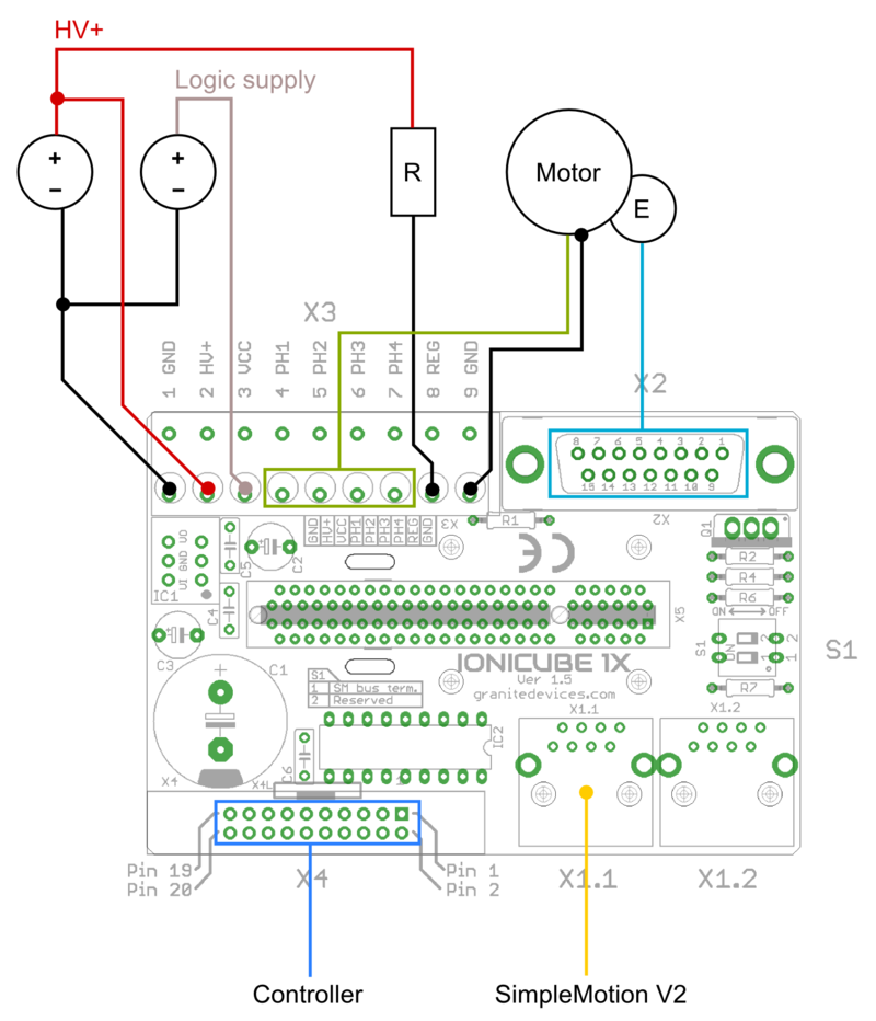
Wiring overview. R is regenerative resistor and E is encoder. In minimum working connection, wire 5V voltage to ENABLE and STO2 inputs into X4 pins (these two signals allow drive to be operated). Note: STO2 accepts voltage from 4.5 to 25 VDC but other digital inputs, such as ENABLE only between 2.7 to 5.5VDC.
| If using switching power supply (SMPS) as motor power supply, external rectifier diodes are needed to protect the power supplies. See See IONI power supply schemes. |
Legend[edit | edit source]
| Color |
|---|
| Supply pin |
| Input pin |
| Output pin |
X3 pinout[edit | edit source]
This is a wire terminal connector for power input and output
| Pin number | Signal name | Usage |
|---|---|---|
| 1 | GND | Ground |
| 2 | HV+ | Motor power supply, HV DC bus (see IONI drive voltage range spec) |
| 3 | VCC | 24V logic supply |
| 4 | PH1 (PHASE1) | Motor phase 1 (see wiring table below) |
| 5 | PH2 (PHASE2) | Motor phase 2 (see wiring table below) |
| 6 | PH3 (PHASE3) | Motor phase 3 (see wiring table below) |
| 7 | PH4 (PHASE4) | Motor phase 4 (see wiring table below) |
| 8 | REG | Regenerative resistor output |
| 9 | GND | Ground |
| Pin number | Signal name | AC/BLDC motor | Brush DC motor | Stepping motor |
|---|---|---|---|---|
| 1 | GND | Ground for cable shield and an optional motor holding brake coil | ||
| 4 | PHASE1 | U (some motors R) | Armature + | Coil A.1 |
| 5 | PHASE2 | V (some motors S) | Armature - | Coil A.2 |
| 6 | PHASE3 | W (some motors T) | Armature - | Coil B.1 |
| 7 | PHASE4 | Not connected | Armature + | Coil B.2 |
Motor & brake wiring schematics[edit | edit source]
Note: the images below are drawn for IONICUBE 4 axis version. IONICUBE 1X wiring is equivalent except there is no brake output in the X3. Brake output pin is located in X4.
| An easy way to verify correctness of two phase stepper connection: unplug the 6 pin connector and then measure resistance between phases 1-2 and 3-4. Multimeter should show the same resistance for both cases (typically 0.1 - 5 ohms). Also when measuring between phases 1-3, 1-4, 2-3 and 2-4, the multimeter should indicate open circuit. |
Regenerative resistor[edit | edit source]
Regenerative resistor is optional and may be connected between REG and HV+ terminals. The on board transistor is capable of carrying max 10 Amp current on regenerative resistor, so minimum allowed resistance can be calculated from: Rmin=HVvoltage/10. I.e. with 48VDC HV supply, the minimum resistance is 48V/10A = 4.8 Ohms. Suggested resistor power capability is 20-100 W.
| When multiple IONICUBE 1X's are connected to a shared HV supply, then it is typically sufficient to have regenerative resistor only in one IONICUBE 1X as it will help to prevent voltage build-up in the HV supply line. |
X2 pinout[edit | edit source]
X2 is the feedback device connector of motor
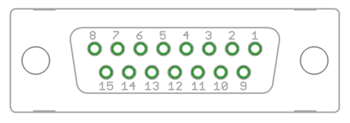
| Pin # | Pin name | Electrical type (in most feedback device modes) | Quadrature encoder | SinCos encoder | BiSS-C encoder | SSI encoder | AMS SSI encoder |
|---|---|---|---|---|---|---|---|
| Shell | GND | Earth/case | |||||
| 1 | HALL_W | Hall sensor digital input, phase W | - | - | - | ||
| 2 | HALL_V | Hall sensor digital input, phase V | - | - | - | ||
| 3 | HALL_U | Hall sensor digital input, phase U | - | - | - | ||
| 4 | GND | Encoder supply ground | |||||
| 5 | B- | Differential input B- | Channel B- | SinCos input B- | - | - | - |
| 6 | B+ | Differential input B+ | Channel B+ | SinCos input B+ | - | - | - |
| 7 | A- | Differential input A- | Channel A- | SinCos input A- | - | - | - |
| 8 | A+ | Differential input A+ | Channel A+ | SinCos input A+ | - | - | - |
| 9 | 5V_OUT | Encoder supply 5V output | |||||
| 10 | GND | Encoder supply ground | |||||
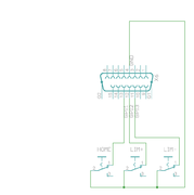
| 11 | GPI3 | Axis negative direction end limit switch (optional). Normally closed (NC) switch is highly recommended for safety reasons. Connect it between this pin and GND pin. Normally open (NO) switch can be used, and the switch polarity can be changed with Limit switch polarityLSP. |
Clock/MA- | Clock- | CLK | ||
| 12 | GPI2 | Axis positive direction end limit switch (optional).Normally closed (NC) switch is highly recommended for safety reasons. Connect it between this pin and GND pin. Normally open (NO) switch can be used, and the switch polarity can be changed with Limit switch polarityLSP. |
Clock/MA+ | Clock+ | CSn | ||
| 13 | GPI1 | Axis home switch switch (optional). Normally closed (NC) switch is highly recommended for safety reasons. Connect it between this pin and GND pin. Normally open (NO) switch can be used, and the switch polarity can be changed with Home switch or hard stop search direction (Home switch polarity)HMS. |
DO | ||||
| 14 | C- | Differential input C- | Index channel Z- | Index channel Z+ | Data/SLO- | Data- | - |
| 15 | C+ | Differential input C+ | Index channel Z+ | Index channel Z+ | Data/SLO+ | Data+ | - |
| Pin layout | Female D-sub 15 connector as it appears from outside of drive. Note: counterpart (male) connector has mirrored pin layout if viewed from pin side, and same layout if viewed from soldering side. | ||||||
| Especially with long encoder cables, it might be necessary to add encoder line termination resistors, see Terminating differential encoder lines. |
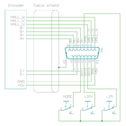
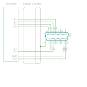
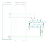
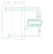
Examples of feedback device and switch wiring[edit | edit source]
| In case of single-ended encoder, connect encoder's A, B, Z only to drive's A+, B+ and C+ and leave drive's A-, B- and C- unconnected. |
| With differential Hall sensor (which provides U+, U-, V+, V-, W+ and W-, connect only sensor's U+, V+ and W+ to drive's HALL_U/V/W. |
| Never connect sensor negative outputs (A-/B-/C-/U-/V-/W-) to GND. Connect them to drive's A-/B-/C- or leave unconnected. |
| Feedback devices with differential signaling may use varying naming schemes of signal pairs. For example differential signal X (which contains two electrical wires) may be denoted as: X+ and X-, or X and \X or X and X. In this Wiki we mark them X+ and X-. Some Fanuc encoders have quadrature signals named as PCA, /PCA, PCB, /PCB, PCZ and /PCZ which are equivalent to A, B and Z signal pairs. |
X4 pinout[edit | edit source]
| This section is unfinished. Don't use until this notice is removed. |
X4 is main control and setpoint signal port consisting Enable input signal, Fault output signal, pulse and direction/quadrature/PWM setpoint inputs and digital outputs for home switch status. X4 is directly wired to conform most common parallel port style pulse & direction CNC controllers.
| Pin number in header | Signal name | Typical usage | Signal name | Typical usage | |
|---|---|---|---|---|---|
| 1 | GND | Ground | 2 | 5V_OUT | 5V output for optional external circuity |
| 3 | HSIN2 | Depending on setpoint mode, can be either:
|
4 | HSIN1 | Depending on setpoint mode, can be either:
|
| 5 | ANAIN+ | +/-10V analog setpoint input2 | 6 | ANAIN- | +/-10V analog setpoint input2 |
| 7 | GPI2 | Enable positive feed (also in X2)1 | 8 | GPI1 | Home switch input (also in X2)1 |
| 9 | GPI4 | Clear faults1 | 10 | GPI3 | Enable negative feed (also in X2)1 |
| 11 | REGEN_OUT | Regenerative resistor power switch state (redundant, IONICUBE 1X has internal power switch) | 12 | GPI5 | Start homing1 |
| 13 | MECH_BRAKE_OUT | Mechanical holding brake output3 | 14 | GPO5 | Reserved for future use1 |
| 15 | GPO4 | Limit switch output | 16 | GPO3 | Fault on any axis or E-stop (active low)1 |
| 17 | GPO2 | Tracking error warning1 | 18 | GPO1 | Servo ready1 |
| 19 | STO2 | Safe torque off input (this pin also present in X14) | 20 | ENABLE | Enable drive (with or without chargepump) (this pin also present in X14) |
1) For detailed pin function and alternative functions in various modes, refer to IONI connector pinout
2) Setpoint voltage is measured from the difference of voltage potentials between ANAIN+ and ANAIN-. Both ANAIN inputs must always lie within +/-12V from GND (meaning that controller's zero voltage reference, i.e. GND must be connected to the GND if drive to prevent voltage potentials from floating.
3) This output can directly drive a 24V solenoid brake (max 500mA) if VCC is supplied by 24 volts. In such case, connect brake wires between MECH_BRAKE_OUT and VCC.
4) The same pin is routed also to X1 connectors. Use ENABLE/STO2 pins of only either X4 or X1, not both.
| Connect X4 directly only to 3.3V or 5V logic systems. For 24V logic, see chapter below. |
X1 connector[edit | edit source]
X1 connectors are for SimpleMotion V2 bus which is used for drive configuration with Granity software and control over a multidrop capable serial data link. For pinout, see SimpleMotion V2 port.
| Never connect an Ethernet to X1. While it uses similar connector and cabling, it is electrically incompatible with Ethernet. Devices may be permanently damaged by mixing Ethernet and SimpleMotion V2. |
| Do now wire SimpleMotion V2 ports with crossover RJ45 cables (see details). Always use straight/non-crossover patch cables. If unsure about what is the type of your RJ45 cable, don't use it. |
DIP Switch S1 settings[edit | edit source]
On board switch S1 controls the SM bus termination. Set switch 1 to ON position if the IONICUBE 1X devie is the only device in a SM bus OR if it's the last device in device chain. All other cases, leave it OFF (in other words, if IONICUBE is chained to multiple SM bus devices and it's not the last device of the chain).
Using 24 Volt control signals[edit | edit source]
As many industrial environments use 24V signaling for logic, interfacing IONICUBE 1X has been designed to accept these voltages with help of external circuits:
- The GPOx outputs are NPN open collector type the pulling pin to GND when output is logic 1. GPO can be loaded up to same voltage level with logic supply voltage.
- If 24V logic accepts such NPN open collector output, wire directly
- If push/pull type output is needed, wire a pull-up resistor (i.e. 2200 Ohm or higher) between GPOx and 24V voltage
- Inputs are routed directly to IONI input pins that accept up to 5V directly. To extend the range, add a resistor divider network to reduce the voltage to accepted level. I.e. on each pin:
- 470 Ohm resistor from GPIx to GND, and
- 2200 Ohm GPIx to user 24V input signal
- That two-resistor circuit will reduce 24V level logic 1 to an acceptable ~4.2V level, while logic 0 will be ~0V.
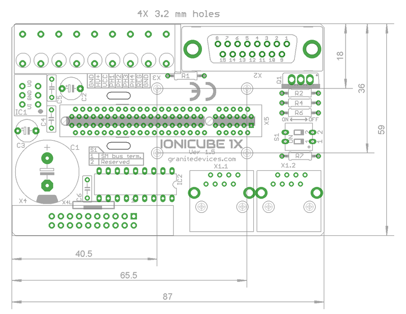
Dimensions and mounting[edit | edit source]
IONICUBE 1X can be mounted by screws to a base or with optional DIN rail clips to a standard DIN rail.
To mount in DIN rail, obtain 2 pcs of Phoenix Contact part number 1201578. Such part is available from many distributors including Digikey 277-2296-ND
.